


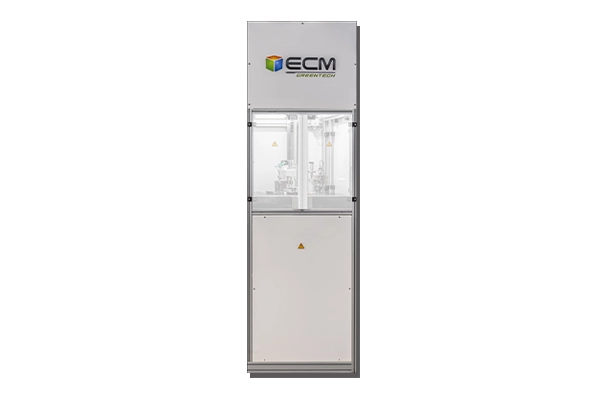
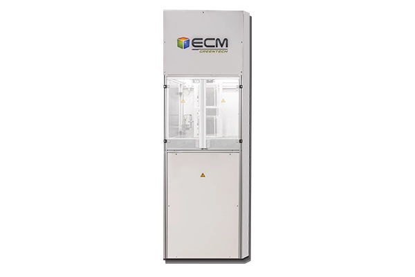
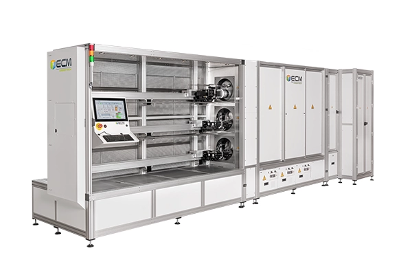
The MEMSLAB compact batch-type, single or multi-chambers vertical PECVD platform offered by ECM Greentech. The MEMSLAB is designed and built with high precision components, which allows for high quality thin film deposition by PE-CVD or PE-ALD. The applied Low Frequency Plasma feature permits the furnace to reach excellent process performance through a most advantageous horizontal thin substrate processing. This platform excels in the processing of various size of substrates at once (from tiny pieces up to 200mm wafers); therefore, allowing the MEMSLAB to meet a wide requirements of universities, research laboratories, pilot production and mass production facilities.
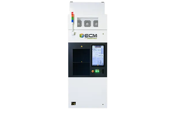
MEMSLAB-UNO – From R&D to Pilot Production
MEMSLAB-SIA – From R&D to Pilot Production
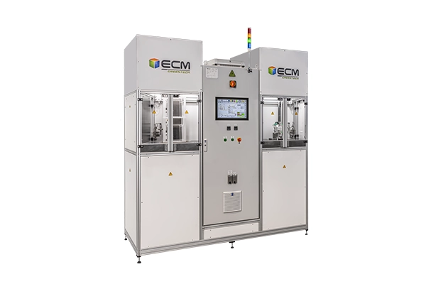
MEMSLAB-DUO – From R&D to Mass Production
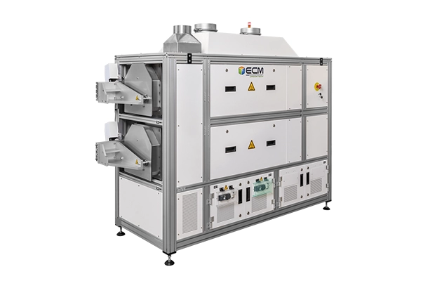
MEMSLAB-TRIO – From Pilot to Mass Production
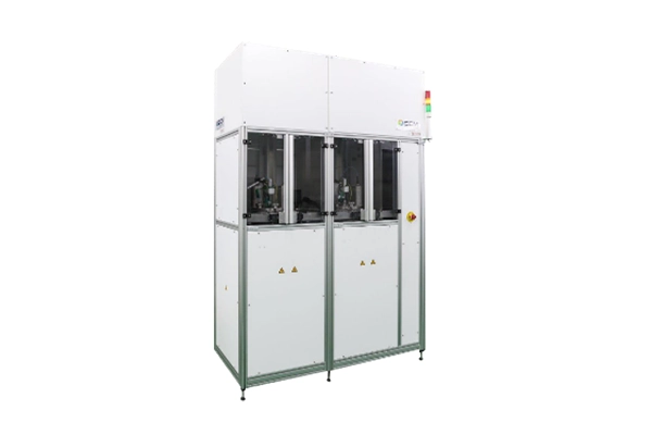
MEMSLAB-QUATRO – From Pilot to Mass Production
Discover all our wafer processing furnaces
Technical Sheet
| Substrate dimensions | Up to 25 wafers per chamber From pieces up to 200 mm semiconductor wafers Alternative graphite plates for multi-size wafers in same batch |
| Substrate material | Si, SiC, GaN, Sapphire, ceramic, quartz, metal (non conductive subtrates upon demand) |
| Features | Modular & Flexible with tiny footprint Excellent process precision and repeatability High performance and life-time process technology Low power consumption and low carbon print Over 30 years process expertise Low RF, Direct Plasma No deposition on reactor walls & vacuum line In-situ cleaning processes Excellent passivation properties Dense layer, good wet chemical resistance Single side deposition or etching Pin mark free Superb deposition uniformity Thin wafer compliant Gas Cabinet for up to 13 gas distribution Multi-Process Gas Panel with up to 9 MFC gas loops |
| Options | Process related pump package SECS/GEM compliant with SEMI E30, E37 Dedicated additional process features upon process configuration In-situ Anneal In-situ cleaning |
| Integration | Cassette to Cassette Automation with Robotic and Wafer Transfer System |
| SiNx |
| SiOx |
| SiOxNy |
| SiCx |
| α-Si (intrinsic or p/n doped) |
| μ-Si (intrinsic or p/n doped) |
| PSG |
| BSG |
| BPSG |
| AlOx |
| More layers upon request |
| In-Situ Cleaning / surface Etching |
'.get_the_title().'
VS Series
VS Series
BATCH TYPE VERTICAL FURNACE
'.get_the_title().'
VAR SERIES
VAR SERIES
BATCH TYPE VERTICAL TUBE FURNACE
'.get_the_title().'
TUBESTAR
TUBESTAR
Batch Type Horizontal Tube Furnace
'.get_the_title().'
MEMSLAB
MEMSLAB
Batch type vertical PECVD – ALD
'.get_the_title().'
ACTISTAR
ACTISTAR
High Temperature Vertical Furnace
'.get_the_title().'
OXISTAR
OXISTAR
High Temperature Vertical Furnace
'.get_the_title().'
DF SERIES